KIMM in MediaKIMM Press Release

[KIMM Press Release] Successful Commercialization of 2D LiDAR Sensors for Semiconductor Wafer Transfer Equipment
- Created2021.08.17
Attached file

Successful Commercialization of 2D LiDAR Sensors for Semiconductor Wafer Transfer Equipment
-KIMM Department of AI Machinery improved the core sensor performance of semiconductor transfer equipment, which is entirely dependent on foreign imports -
-SOSLAB, a professional LiDAR sensor provider, got a green light for commercialization through the acquiring of mass production technology-
The Korea Institute of Machinery and Materials (KIMM, President Sang-jin Park), which operates under the jurisdiction of the Ministry of Science and ICT, together with SOSLAB (Jiseong Jeong, CEO), a professional LiDAR sensor provider, have succeeded in the commercialization of 2D LiDAR sensors that are mounted on equipment for transferring semiconductor wafers.
LiDAR sensors are devices that continuously emit millions of laser beams per second and measure distance based on the time it takes for the laser beams to return to the sensor. These sensors then use this information to identify the surrounding environment threedimensionally. As such, this technology is an essential component for autonomous driving.
The Overhead Hoist Transport (OHT) systems, autonomous operating system that transfers wafers by moving them alongside rails installed on the ceiling, are applied within the semiconductor production lines. Two to four LiDAR sensors are required for single OHT system, and until now, Korea has solely depended on foreign countries, such as Germany and Japan, for the production of such LiDAR sensors.
Dr. Chang-wan Ha, Senior Researcher at the Dept. of AI Machinery, and the research team have cooperated with SOSLAB, a LiDAR sensor production company, and SEMES, an end-user company for such services, to commercialize the LiDAR sensor for semiconductor wafer transfer equipment. Through cooperation, the team has successfully improved the product performance and acquired the mass production technology.
The research team has cooperated with the relevant companies, and started developing the customized products fitted for actual semiconductor production lines. Also, by conducting performance tests together with the end-user company, the team has been able to maximize the reliability of the field application.
Through the product optimization and optical path alignment improvement for mass production, the team has improved the LiDAR sensor’s measurement resolution and accuracy, which are the key functions of the LiDAR sensor. Also, by automating the calibration and performance testing stages after the product assembly, the team has acquired the technology for mass production.
This technology is expected to replace the annual imports of about 4,000 units of 2D LiDAR sensors for semiconductor wafer transfer equipment, based on the end-user company demands. In addition, it is expected to be applied in the development of various LiDAR sensors in the future, for the establishment of autonomous driving, smart mobility, and smart infrastructure.
Dr. Ha stated that it is a meaningful opportunity for government-funded research institutes, domestic companies, and companies demanding services to actively cooperate in the localization of products that had, up until now, been characterized by a dependency on foreign imports. He added that, through this development, it will be possible to more stably protect the domestic semiconductor ecosystem from changes in the external environment, such as Japan’s tightening of export regulations.
Jiseong Jeong, the CEO of SOSLAB, also expressed his gratefulness for having this opportunity to contribute in strengthening the national technological power. He further stated that the company will do its best to become the world’s best LiDAR sensor provider within the autonomous driving and smart infrastructure markets.
[List of Attachments] - Attachment 1: 2D LiDAR sensor for semiconductor wafer transfer equipment (photo)
- Attachment 2: Semiconductor wafer transfer equipment (OHT) (photo)
The Korea Institute of Machinery and Materials (KIMM) is a non-profit governmentfunded research institute under the Ministry of Science and ICT. Since its foundation in 1976, KIMM is contributing to economic growth of the nation by performing R&D on key technologies in machinery and materials, conducting reliability test evaluation, and commercializing the developed products and technologies.
These R&D results were carried out as a project for the performance improvement and mass production technology development for 2D LiDAR sensors used in semiconductor wafer transfer equipment. This project was promoted as part of the material, parts, and equipment mass production performance evaluation support project under the Korea Institute for Advancement of Technology (KIAT).
Credit : The Korea Institute of Machinery and Materials (KIMM)
Usage Restrictions of Multimedia (Attachment File) : The sources of photos and research results from KIMM must be specified.
- Attachment 1: 2D LiDAR sensor for semiconductor wafer transfer equipment (photo)
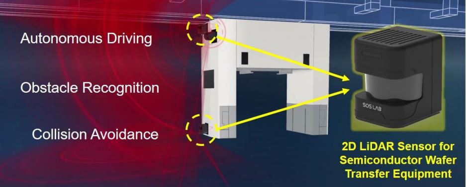
Photo description: The 2D LiDAR sensors are attached to the semiconductor wafer transfer equipment (OHT). These 2D LiDAR sensors are essential parts in the system and act as the eyes of the autonomous driving system; the sensors recognize the surrounding environment three-dimensionally and are in use for obstacle recognition and collision avoidance.
- Attachment 2: Semiconductor wafer transfer equipment (OHT) (photo)
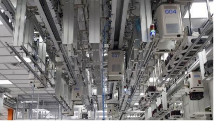
Photo description: The photo of newly developed 2D LiDAR sensors for semiconductor wafer transfer equipment. This photo shows the semiconductor wafer transfer equipment (OHT) with 2 to 4 LiDAR sensors attached to each equipment.
Attached file
