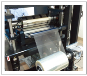
Micro or nanoscale mask is amounted on thermal-roll imprinting
system to place pressure and heat to the lower roll to directly create
micro patterns on flexible/elastic plate; and device manufacturing
method using this technology
Client / Market
- Transparent electrode, optical film, protection film, next generation display, bio
sensor, Microlens, membrane plate, 3D sensor, energy device and wave absorber, etc.
- Roll-to-roll and roll-to-plate printer’s functional micro plate and hybrid device ma
Necessity of this Technology
- Existing imprint and hot embossing process technology does not directly engrave
on the flexible plate but imprint on photo register or resin and go through secondary
and tertiary processes such as development and etching to make the device.
- It requires a lot of equipment, great cost, and many process stages.
- The technology cannot be applied for a roll.
Technical Differentiation
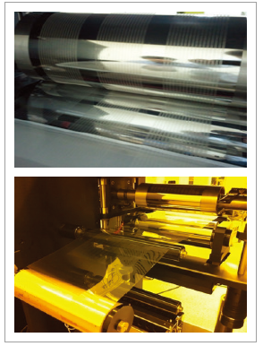
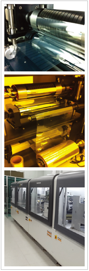
- With the roll-to-roll method, micro pattern is directly engraved on a flexible/elastic plate.
- Possible to make a device using one device with the pattern imprinted on a flexible
plate and coating process
- Possible to applied to micro/nano pattern printing technology
- With roll-to-roll/roll-to-plate method, micro pattern is directly imprinted on a
flexible/elastic plate – significantly reduces the number of steps.
- Possible to freely imprint micro and nano-sized patterns using a flexible metal mask
- Possible to achieve high imprint rate using heat and pressure press roll
- The line width is more consistent compared to patterning from existing printing and
imprint process (outstanding optical property)
- No limits regarding materials to be used as various types of flexible (PET, PEN, PC,
etc.) and elastic materials can be used.
Excellence of Technology
- In foreign countries, nano technology-based imprinting technology is actively
utilized in display, biosensor, and semiconductor markets, and nano imprint
device market has been growing 40% each year from 55 million USD in 2006 and is
expected to reach 2.2 billion USD in 2018. (Source: BCC Inc, 2005)
- In overseas markets, next generation display has been showing annual average
growth rate of 20% since reaching 6.8 billion USD in 2009; it is expected to hit 16.9
USD in 2014. (Markets and Markets, 2009)
- The size of the world biosensor market is expected to expand from 6.7 billion USD in
2009 to 14.4 billion USD in 2016, and the accumulative annual average growth rate
from 2009 and 2016 is estimated to be 11.6%. (Frost & Sullivan, 2010)
- Locally, the industry is focusing on nano imprint technology development around
the field of display.
- A domestic nano imprint device manufacturer NDD has conducted a test on nano
imprint commercialization jointly with another display manufacturer, and Minuta
Tech, subsidiary of Techno Semichem, has developed molding material for nano
imprint. Applied research on OLED, organic solar cell, and next generation small
storage medium are being actively conducted.
- As thermal engraving device or roll-to-roll thermal engraving device for prototype
production, there are few sizes other than 5000×1500×2000 mm, resolution
between 60 nm and 20 μm, and the film width between 300 and 100 mm. The device
is used for creating a device for transparent electrode, protection film, optical film,
TSP, NFC, OPV plate, energy storage, and current collection.
Current Intellectual Property Right Status
PATENT
- Printing Device Using Thermal Roll Imprinting and Patterned Plate and Microfluidic
Device and Film Laminating Device for Sensor and Printing Method Using the Printing
Device (KR1022015, PCT/KR2011/ 002505, EP112010003566.0, US13/394182)
- Roll Imprinting Device (KR0988935, CN201080048087, DE112010004165.2,
US13/499837)
- Film Product Manufacturing Method Using Thermal Roll Imprinting and Blade
Coating, and Protection Film and Electric Device Comprising Film (KR1022015,
US13/582530, EP11766198.3, PCT/KR2011/002505)
- Printing Device Using Thermal Roll Imprinting and Patterned Plate and Microfluidic
Device and Film Laminating Device for Sensor and Printing Method Using the
Printing Device (KR0957622)
- Roll Imprinting Device and Method (KR1552935)
- Roll Imprinting Device (KR0988935, China, Germany, USA)
KNOW-HOW
- Ink/Paste inking and removing technology on engraved flexible/elastic plate
- Flexible/Elastic plate surface treatment technology
- Electrical/Mechanical property assessment technology for flexible/elastic device
- Remolding process technology for consistent imprint
|