
KIMM in MediaKIMM Press Release

[KIMM Press Release] Fast, affordable solution proposed for transparent displays and semiconductors
- Created2021.05.12
Attached file

Fast, affordable solution proposed for transparent displays and semiconductors
-KIMM develops roll-based transfer technique to transferwafer-scale two-dimensional nanomaterialswithout damages -
The Korea Institute of Machinery & Materials (President Sang Jin Park; hereinafter KIMM) under the Ministry of Science and ICT developed a roll-based damage-free transfer technique that allows two-dimensional (2D) nanomaterials to be transferred into wafer scale without damage. The proposed technique has a variety of applications from transparent displays and semiconductors to displays for self-driving cars, and is expected to accelerate the commercialization of 2D nanomaterial-based high-performance devices.
Dr. Kwang-Seop Kim, principal researcher of the Department of Nano-Mechanics at KIMM, succeeded in developing a technique of transferring 2D nanomaterials, as thin as 1/50,000 of a strand of hair, to a substrate of at least 4 inches (approx. 10 cm) without damage.
The roll-based transfer is a process in which 2D nanomaterials on a transfer film are transferred to a desired substrate. It is a highly efficient technique that enables large-area continuous transfer of nanomaterials, similar to paper printing.
The transfer process involves nanomaterials on a transfer film (A) and a target substrate (B). In roll transfer, the nanomaterials are transferred to B when A is rolled onto B. This is similar to the process of transferring a tattoo onto skin using a tattoo sticker. The sticker plays the role of the transfer film, the tattoo represents the 2D nanomaterials, and the skin is the substrate.
The key point in the proposed technique is to identify two different types of the damage mechanisms in relation to the deformation of adhesive layer in the transfer film through computer simulation and experiments. The team optimizes the thickness of the adhesive layer to minimize the deformation of the adhesive layer during the transfer process, leading to achieve the damage-free transfer of large-area 2D nanomaterials.
The team discovered the principle behind the damage-free transfer of an extremely thin tattoo to skin through optimizing the tattoo sticker.
The technique can be utilized in the roll-based transfer process for the production of 2D nanomaterial-based flexible transparent displays and transparent semiconductors, decreasing the damage in 2D nanomaterial down to 1% compared to the existing 30%.
Principal researcher Kwang-Seop Kim said, “Our technique of transferring large-area 2D nanomaterials and micro-devices without damage to substrates will significantly lower manufacturing costs of wearable devices, flexible transparent displays, and highperformance bio/energy sensors, thus accelerating the commercialization of related applications. We also expect to see new businesses across industries from nextgeneration semiconductors to future vehicles.”
[List of Attachments] - Attachment 1: Roll-based damage-free transfer technique for large-area 2D nanomaterials (photos and graphic image)
- Attachment 2: Wafer produced by the roll-based transfer technique for large-area 2D nanomaterials (photo)
- Attachment 3: KIMM’s progress on roll transfer technology research
The Korea Institute of Machinery and Materials (KIMM) is a non-profit governmentfunded research institute under the Ministry of Science and ICT. Since its foundation in 1976, KIMM is contributing to economic growth of the nation by performing R&D on key technologies in machinery and materials, conducting reliability test evaluation, and commercializing the developed products and technologies.
The research was supported by grants under the “Development of Nano-Manufacturing Machine Technology for Flexible and Transparent Displays in Autonomous Vehicles” of KIMM, and “Development of Meta-display Technology based Micro-LEDs,” a Global Frontier R&D Program on Center for Advanced Metamaterials funded by the National Research Foundation, under the Ministry of Science and ICT.
An article explaining the results of this research was published in the May issue of NPG Asia Materials, a journal published by the Nature Publishing Group, under the title of “Damage-free transfer mechanics of 2-dimensional materials: competing between adhesion instability and tensile strain.”
Credit : The Korea Institute of Machinery and Materials (KIMM)
Usage Restrictions of Multimedia (Attachment File) : The sources of photos and research results from KIMM must be specified.
- Attachment 1: Roll-based damage-free transfer technique for large-area 2D nanomaterials (photos and graphic image)
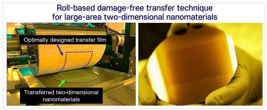
Photo description: Dr. Kwang-Seop Kim and his research team at the Department of NanoMechanics, KIMM, have succeeded in developing the roll-based damage-free transfer technique for 2D nanomaterial (monolayer graphene)
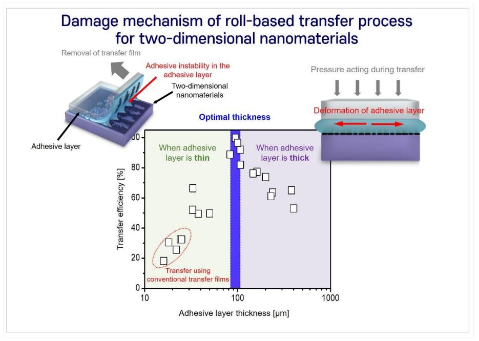
Image description: Dr. Kwang-Seop Kim and his research team at the Department of NanoMechanics, KIMM, have revealed a damage mechanism of roll-based transfer process for 2D nanomaterials. If the adhesive layer is too thin, damage occurs to the 2D nanomaterials from adhesion instability; and if the adhesive layer is too thick, the contact pressure during the transfer process causes excessive deformation, causing damage to the materials.
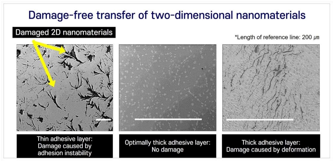
Image description: Dr. Kwang-Seop Kim and his research team at the Department of NanoMechanics, KIMM, have succeeded in designing a transfer film with an optimally thick adhesive layer, and applied it to the roll-based transfer process to successfully transfer 2D nanomaterial (monolayer graphene) to the desired substrate without damage.
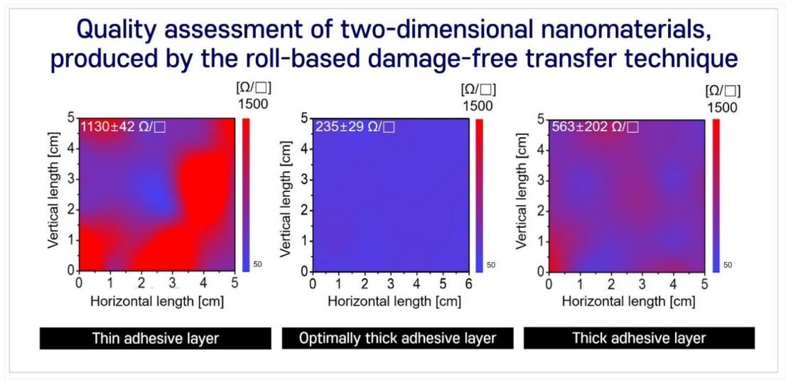
Image description: A graph showing the sheet-resistance quality of 2D nanomaterial (monolayer graphene) based transparent electrodes, produced by the roll-based transfer technique. The lower the sheet resistance, the better it conducts electricity to transparent electrode (monolayer graphene); and the more uniformed the sheet resistance quality, the better one can make large-scale transparent electrode.
When the adhesive layer is thin, the sheet resistance is extremely high at 1130 Ohm/sq., and the sheet resistance quality is non-uniform. When the adhesive layer is thick, the sheet resistance is 563 Ohm/sq., and the sheet resistance quality is again non-uniform. When using the transfer film designed to have an optimally thick adhesive layer, the sheet resistance is very low at 235 Ohm/sq., and the sheet resistance quality is uniform.
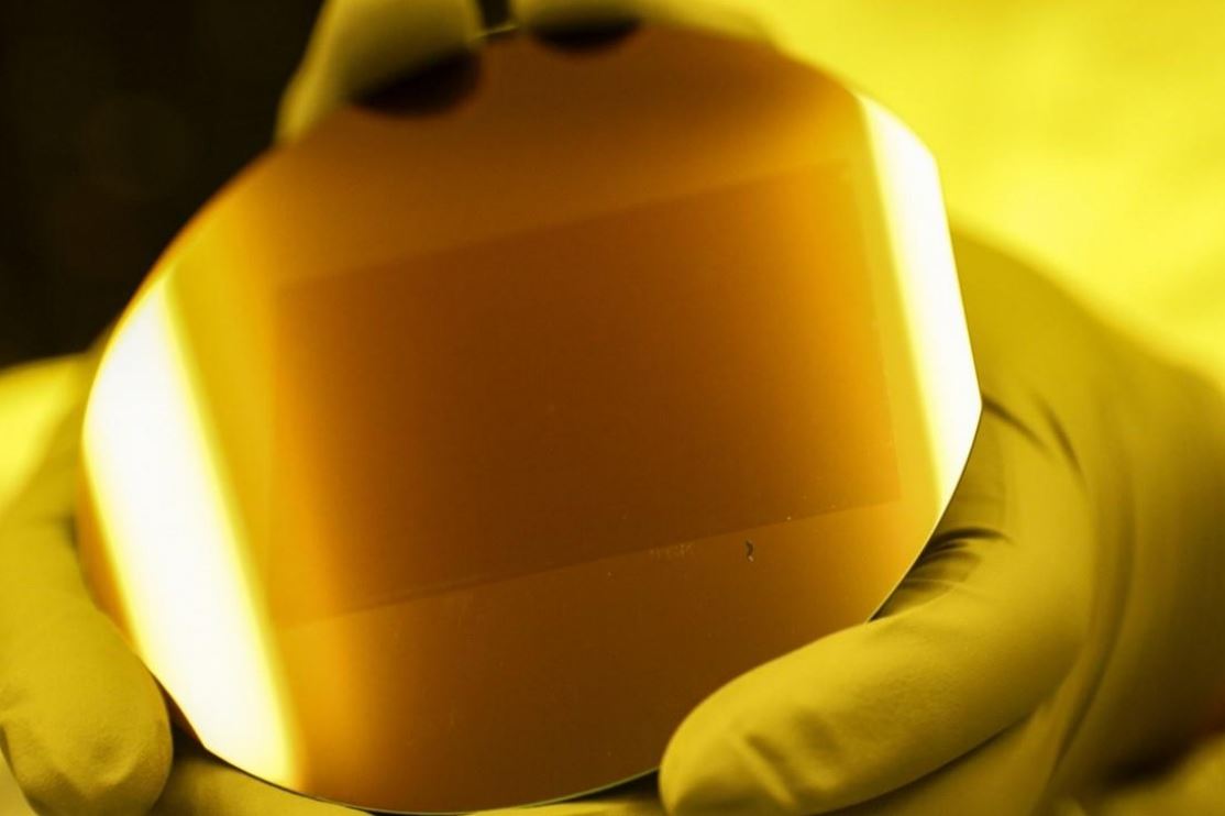
Photo description: The wafer produced by Dr. Kwang-Seop Kim and his research team at the Department of Nano-Mechanics, KIMM, using the roll-based damage-free transfer technique for 2D nanomaterials.
- Attachment 3: KIMM’s progress on roll transfer technology research
The Department of Nano-Mechanics at KIMM has been researching on the roll-based transfer technology for more than ten years.
The department developed roll transfer technology for easily breakable thin-film transistor (TFT) devices using patented technology in 2013, and secured roll transfer-based singlecrystal silicon memory device manufacturing technology in 2016. It also acquired microLED (light-emitting diode) stretchable display technology based on roll transfer in 2017
Four patents related to mini-LED roll transfer were issued following the establishment of YTS Micro-Tech, an institute-affiliated company, in 2019. Recently, YTS Micro-Tech succeeded in expanding the 4-inch roll transfer technique to 10-inch scale, and is actively developing mini-LED BLU (back light unit) for smartpads.
Also, when the Center for Advanced Meta-Materials – organizer of the Global Frontier Program – established the MCK Tech Co., Ltd. in 2019, the department registered four jointly owned patents related to roll-based graphene synthesis and transfer. MCK Tech Co., Ltd. is utilizing large-scale 2D nanomaterial synthesis and transfer techniques in the development of transparent electrodes for smartphones and graphene biosensor applications.
The damage-free roll transfer technique developed for 2D nanomaterials in this research is expected to create a new paradigm in semiconductor and display markets.
Attached file
