Developing a new concept for High device performance/high flexibility
The formation of Fine metal patterns(≤100 μm)for FHE(flexible
hybrid electronics) and the fabrication of 3D step height metal
interconnection
DI(direct imaging) technology for creating non-damaging fine
pattern(≦100 μm)/pitch(≦20 μm) for stretchable device and display
Client / Market
- Technical field for FHE (flexible hybrid electronics)
- Technical field for DI (direct imaging) fine pattern/pitch formation for non-damaging
flexible/stretchable display areas
Necessity of this Technology
- When using existing mass production MEMS Fab. process/equipment, the process
cannot be performed if there is step height (≧5 μm) between the substrate and the
thin chip (equipment / process compatibility issue).
- n forming 3D interconnection, wire-bonding creates mechanical damage of less
than 50 μm to the thin chip due to heat, pressure, and ultrasonic energy.
- Absence of face-up 3D metal interconnection technology to fabricate fine pattern (≦
100 μm) pitch (≦20 μm)
- Absence of technology that can form flexible/stretchable pattern without damaging
low Tg flexible/stretchable substrate (wiring printing and sintering technology)
- Therefore, to overcome such problems, it is necessary to develop DI type nondamaging
fine pattern/pitch creation technology.
Technical Differentiation
- Technology to effectively form 3D interconnection masklessly without causing
mechanical damage to the thin chip with thickness below 50 μm mounted on the
flexible/stretchable substrate
- Technology to create fine pattern (≦100 μm)/pitch (≦20 μm) with the DI (direct
imaging) method
- Technology to sinter ink material on the flexible/stretchable substrate without
thermal damage
- Technology for intrinsically/geometrically robust metal pattern formation for
stretchable display
- Technology to rework and repair for mass production yield improvement
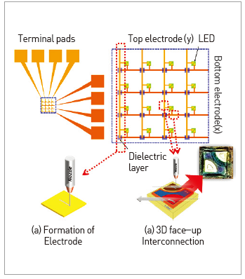
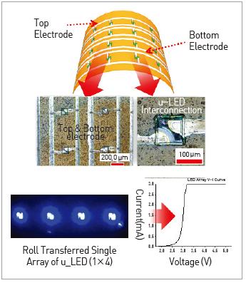
Excellence of Technology
- Formation of 100 μm×100 μm (thickness≈5 μm) micro-LED top & bottom electrodes
and securing face-up 3D metal interconnection (line width ≦ 30 μm)
- Securing DI micro metal pattern method when line width is below 10 μm
- Establishment of database by ink material for overcoming 3D step height in the flat (0 μm)
to 50 μm area
- Securing sample production technology for micro step height (flat (0 μm) to 50 μm)
control for DI process and ink property evaluation
- Performance of laser sintering test for non-damaging ink sintering on polymer
substrate
Current Intellectual Property Right Status
PATENT
- Wearable Dry Patch Type Hybrid Substrate and Manufacturing Method (KR1756847)
- Non-penetrating, Superhydrophobic Polyimide Film Manufacturing Method
(KR1641207)
- Elastic Device Manufacturing Method and Elastic Device Manufactured with the
Method (KR2017-0133265)
- Electrode Pattern Formation Using Laser Sintering and Electrode Pattern Formation
System for the Method (KR2017-0060814)
KNOW-HOW
- Non-damaging, DI fine pattern/pitch formation technology
- Face-up 3D step-covered metal interconnection technology
- Intrinsically/geometrically flexible or stretchable metal formation technology
- Repair and maskless process technology for yield improvement
|