Interconnection/stacking technology for ultra-thin flexible
semiconductor package with flexible substrate using polymer
elastic bump, neutral plane design for package
Client / Market
- Semiconductor manufacturer (Foundry, OSAT (Outsourced Semiconductor Assembly and Test))
- Display manufacturer
Necessity of this Technology
- Along with development of wearable device performance and rapid growth of its
market, the need for ultra-thin, high-performance, high-flexibility, and humanfriendly
flexible semiconductor package has increased.
- To create a flexible semiconductor package, a thin silicon chip with the thickness
between 20 to 50 μm needs to be bonded on a flexible substrate.
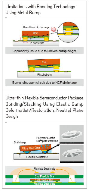
- Conventional bonding process using solder bump to bond the chip under high
temperature has a problem of flexible substrate damage and thin silicon chip
damage due to thermal stress.
With another bonding technology, a rigid metal bump can be bonded with a pad
using NCF adhesive, however, it leads to issues such as chip damage due to
stress concentration caused by uneven bump height, joint coming off due to NCF
shrinkage, and declined flexibility due to hard joint.
Technical Differentiation
- This technology uses the wafer transfer technology to design the neutral plane for
the chip to minimize stress while bending and make handling chip during bonding
easy to enable production of ultra-thin flexible silicon chip that is thinner and more
flexible than the conventional chip.
- By applying the polymer elastic bump structure, which boasts easier elastic
deformation and restoration, for the thin flexible silicon chip, damage to the thin
flexible chip from uneven bump height during chip bonding is minimized with the
elastic deformation and stress relaxation.
- Also, this bonding technology has excellent reliability and low contact resistance as
the contact between the bump and the pad is maintained with the elastic restoration
even when the adhesive shrinks. With the flexible bonding interface composed
of polymer bump and adhesive, this technology is able to realize higher flexibility
compared to conventional bonding technology.
Excellence of Technology
- With wafer transfer technology, neutral plane for chip/package is designed to allow
handling and bonding of thin flexible chip with thickness less than 10 μm without damage.
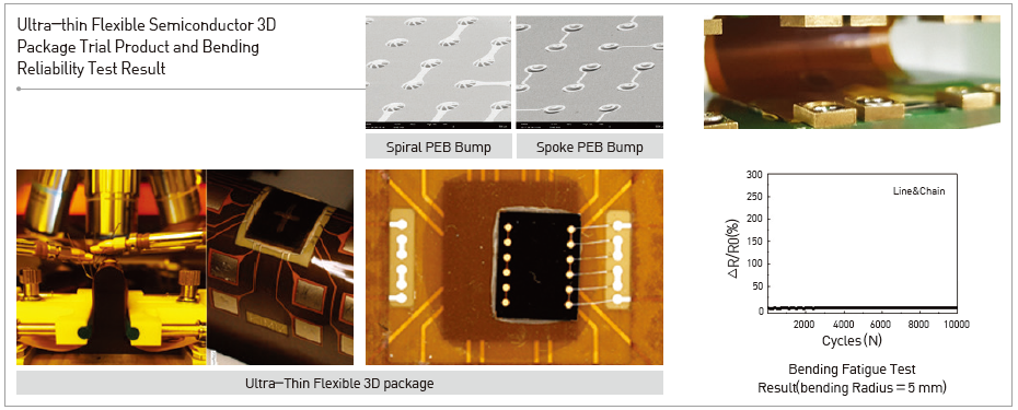
- By applying the polymer elastic bump structure that boasts easy elastic deformation
and restoration to thin flexible silicon chip, a flexible semiconductor package with
bending radius of 5 mm and bending fatigue of over 10,000 cycles was created.
- Using the bonding technology above, the 3D ultra-thin flexible semiconductor
package trial product was manufactured to prove the technology.
Current Intellectual Property Right Status
PATENT
- Face-down Type Flexible Electronic Device Manufacturing Method and Flexible
Electronic Device Manufactured Using the Method (KR1511023)
KNOW-HOW
- Polymer elastic bump fabrication technology
- Flexible chip neutral plane design and thinning technology
- Thin wafer transfer technology for neutral plane design
- Flexible semiconductor package 3D stacking and low-temperature bonding technology
|