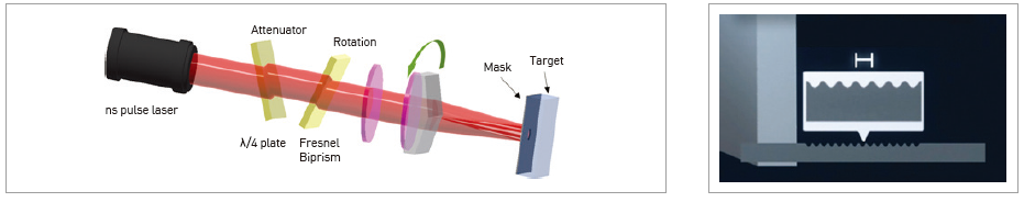
With the micro patterning technology using laser intervention, the
technology enables direct machining on various materials including
metal surface with pulse laser.
Client / Market
- Laser manufacturing equipment
- High-speed micro pattern maker users (e.g. anti-forgery pattern making, pattern
making for catalyst contact area increase for fuel cell or solar cell)
Limitation of Existing Technology
- Existing focus type laser machining has limits regarding diffraction that machining
of small patterns is difficult and the machining time is long due to stage moving, etc.
- Research on laser intervention machining is being conducted to overcome the
problem of above focus type laser machining, however, the research is limited
to continuous wave laser with excellent coherency that it can only be applied to a
photosensitizer.
- Therefore, a high-speed micro patterning technology that can be directly applied for
various materials–metal surface, in particular–is demanded.
Technical Differentiation
- Passible to perform one-shot patterning onto a large area–high-speed patterning
with the speed of 5 n sec
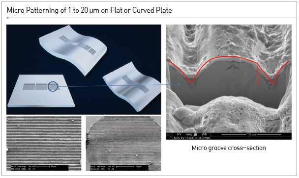
- Possible to create micro patterns with the pattern pitch size between 1 and 20 μm
- Possible to perform patterning on all materials where the surface can be polished
including metal surface
Excellence of Technology
- High-speed, large-area patterning technology is expected to shorten the
processing time approximately up to 100 times compared to the existing method.
- Possibility of creating very small line or dot patterns with the pattern pitch size
between 1 and 20 μm has been confirmed.
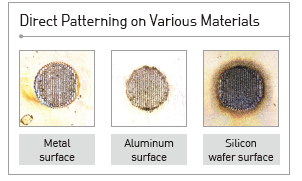
- Pattern making with this technology on various materials including metal,
aluminum, and silicon wafer surface has been verified.
- The optical system can be easily rotated that it can create a line pattern with
different column direction continuously at a high speed.
- Patterns generated with this method can be matched according to the serial
number to be used for anti-forgery.
- A repetitive pattern can be created on a roll or curve by using this technology.
Current Intellectual Property Right Status
PATENT
- Anti-forgery Pattern Generating Device (KR1764835)
- Anti-forgery Pattern Generating Device and Method (KR1688613)
- Anti-forgery Pattern Detection Device (KR1685617)
- Anti-forgery Pattern Detection Device and Method (KR1597754)
- Anti-forgery Pattern Generation Device and Method (KR1528345)
KNOW-HOW
- Synchronization technology for pulse laser, rotary optical system, etc.
- Pattern commissure precision machining technology
|