Laser technology is able to realize electrodes (seed) on a curved or
complex-shaped surface and produce micropatterns stably with a
size under 20 microns using electroless plating
Client / Market
- PCB-based electronic components, automobile industry
- Plastic-based manufacturing industry
Necessity of this Technology
- Recently, the field of printing technology is expanding from 2-dimensional flat
surfaces to 3-dimensional spaces, but a patterning technology on printed-curvedsurfaces
is yet to be realized.
- For existing technologies including photolithography and printed electronics, various
technologies have been developed based on planography, but due to fundamental
technical limitations, it is impossible to print on the complex shaped-surfaces such
as a curve.
- Also, there are issues such as the cost rise from a material waste, the increase
in investment for complex processes, the environmental pollution problem from
chemical processes, and low printing quality due to technical limitations.
- The new technology aims to expand the possible printing area, improve printing
quality, reduce high production cost, and realize an eco-friendly process.
Technical Differentiation
- As the printing area is expanding using a high-performance laser, patterning can be
done on a 3D structures that have curve or other complex shapes such as electronic
clothes. New products can be developed and released.
- With the benefits of laser-high reproducibility and consistency, the highly stable
printing technology can be achieved, resulting in great reduction of the defect rate.
- By minimizing the use of consumable materials such as various solutions and inks
used for chemical processes, the cost of process can be reduced down to 20% in
comparison to the current process cost.
- As the chemical process is minimized, the polluted wastewater can be significantly
reduced and an Eco-friendly technology can be realized.
- As it enables realization of complex patterns, more freedom is given in terms of
designing electronic circuits or components. As a result, it is also favorable for
customized productions and small quantity batch productions.
- Existing technology only allowed plane-to-plane patterning, but with this
technology, the focus of the laser can be adjusted to enable precise patterning on
surface of any kind of shape (even complex surfaces).
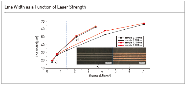
- An existing printed electronics method has serious problems. Uneven line width and
short circuit can be occurred for micropatterning. However, this laser technology
will able to achieve less than 20 μm of micro line width and uniform the width of line
width with high quality.
- The process is based on the direct patterning which is consisted of two stages; seed
generation with laser irradiation and electroless plating. Therefore, the process is
significantly simple and stable.
Excellence of Technology
- This technology is a type of LDS (laser direct structuring) patterning method whose
key factors are the high-performance laser and photo-reactive insulation material.
- High-performance laser should be able to pattern with a consistent line width. The
photo-reactive material should be metallized after react with the laser, and act as a
plating seed (aluminum) for electroplating.
- By exhibiting this technology at ‘Nano Korea 2012’ with the company that
participated in the technology development, the excellence of the technology was
proven.
- The senior researcher has over 20 years of research experience.
Current Intellectual Property Right Status
PATENT
- Manufacturing System of Flexible Printed Circuit Board using Laser and
Manufacturing Method Thereof (KR1377273)
- Flexible Printed Circuit Board Having Conductive Circuit Pattern by Laser Direct
Writing Method and Manufacturing System and Method Thereof (KR0906408) and
Others
|