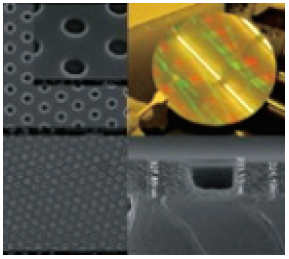
It is technology for continuously transfer nanopatterns on 6-inch
size Si wafer and/or flexible substrates by the liquid transfer imprint
lithography process using the multi-layer nanoimprint lithography
systems

Client / Market
- Flexible electronic devices, displays, solar cells, WGPs
Necessity of this Technology
- Conventionally developed multi-layer nanoimprint system can perform waferbased
nanoimprint process that it uses a stamp with nanopatterns, cure the
coated UV/Thermal resist by means of UV and heat sources. It can be done up to
8-inch substrate. The minimization of the residual layer thickness for a large area
substrate is required absolutely.
- In order to minimize the residual layer thickness in the nanoimprint lithography
process, the liquid transfer process is required.
- In order to do the next additional process after nanoimprint process, etching
process is inevitably required to eliminate the residual layer. There are many studies
to minimize the residual layer thickness, so far.
Technical Differentiation
- As the result of experiments, almost 50% of the polymer applied on the donor side
could be stripped off that compared to existing nanoimprint process, the thickness
of the residual layer could be reduced significantly, which means etching is almost
unnecessary and realization of follow-up process is made easy.
- We are able to do the nanopattern transfer to the substrate with very low applied
load on the stamp side by the line or tiny plane contact conditions because of the
roll-shaped stamp.
- Liquid transfer type roll nanoimprint process uses the roll-shaped stamp to strip off
the polymer applied on the donor side at a uniform thickness and transfers on the
acceptor side, which is similar to the inking process, but is very different in a sense
that it can transfer nanopatterns and transfer polymer in multiple layers using UV.
- Resist on the donor side is supplied through the spin coating process, and it peeloff
using the soft material stamp is transferred to the acceptor side. The pattern
transferring is able to do on the acceptor side even the surface is non-flat or lower
uniformity.
- Unlike existing nanoimprint process, the thickness of residual layer can be reduced
significantly, which means etching is not necessary and realization of follow-up
process is made easy.
Excellence of Technology
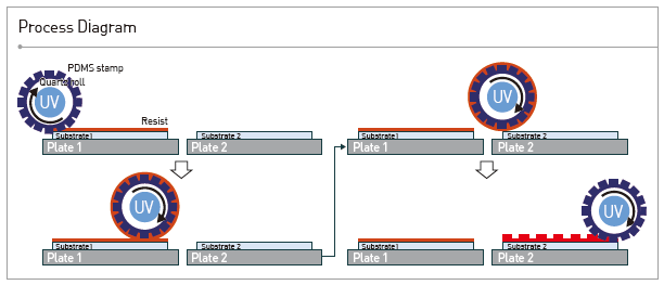
- In the process of transferring the resist applied on Plate 1 with the roll-shaped
stamp and retransferring it to Plate 2, the surface pattern on the roll-shaped stamp
is copied onto the resist applied on Plate 2, and this enables stable performance of
liquid transfer nanoimprint process on a large plate or flexible plate.
- IThere is the donor side station that continuously supplies resists by means of
spin-coating process and the acceptor side station where nanopatterning process
happens using the peel-off resist from the donor side. The resist is peel-off using
a roll-shaped material stamp in the donor side and moved to the acceptor side
station to transfer the peel-off resist with UV light source.

Current Intellectual Property Right Status
PATENT
- Apparatus and Method for Liquid Transfer Imprint Lithography Using a Roll Stamp
Method (KR1303194, PCT/KR2013/012297)
- A Construction/Separation Type Individually Actuating Imprinting Apparatus
(KR585951)
- Imprinting Apparatus for Making Uniform Contact Between Stamp and Wafer and/
or Substrate (KR784827)
- Individually Actuating Nanoimprint Lithography Apparatus (KR1093820)
- Continuous Nanoimprint System Using Rotatable Angulated Roll Stamp (KR1238628)
- Nanoimprint Apparatus and Nanoimprint Method (KR1299919)
- Roll Stamp Manufacturing Apparatus and Roll Stamp Manufacturing Method and
Clone Stamp Manufacturing Stamp Using the Apparatus (KR1332323)
- Nanoimprinting Lithography Apparatus Using Roll Stamp (KR784826)

|


