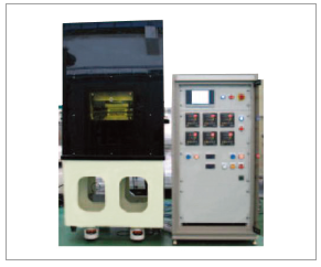
Nano-microscale patterning technology on more than 6-inch
substrates.
Client / Market
- Display manufacturer, flexible plate device manufacturer, Si solar cell and thin film
solar cell manufacture, nano/bio device field and nano-manufacturing systems
company
Necessity of this Technology
- Technology of an apparatus for patterning on a 6-inch wafer or flexible polymerbased
substrate has been developed, but there is no any automated system
technology that includes the ability to automatically and/or continuously feed
substrates
- Suss Microtec in Germany and EVG in Austria have developed and commercialized
the high temperature thermal-nanoimprint systems.
- These technologies have some limits, for example, the large diameter or width
substrate and the stamp materials because it developed use for only some silicon
wafers under vacuum environments condition in order to get rid of entrapped
air bubbles between the stamp and the substrate. In the case of vacuum-based
system, there are some problems to control the applied pressure.
- The nanopatterning process is not able to perform continuously by changing the
stamps i.e. roll-shaped stamps and the substrates, and the extendibility of the
systems is very low.
- Therefore, this technology could be overcome the limitations regarding the flexible
stamp and enhances the pattern uniformity on the large area substrates.
Technical Differentiation
- It can be applied in various filed, because it has more various types of stamp or
flexible stamps i.e. Ni, Si, Glass, PMMA, PC, PET can be utilized compared to existing
apparatus. Also, the its extendibility can be enhanced through loading and unloading
the flexible plate and adjustment of heating/cooling plate size to be applied for
various research areas.
- By enlarge the heating/cooling plates, it can be performed on a large area up to 8
inches, and over 95% of pattern uniformity can be achieved for 50 nm pattern on the
polymer coated substrates.
- It can be fabricated on some high aspect ratio nanostructures up to 8 inch substrate
with faster heating and cooling speed.
- It can be applied in various filed, because it has more various types of stamp or
flexible stamps i.e. Ni, Si, Glass, PMMA, PC, PET can be utilized compared to existing
apparatus. Also, the its extendibility can be enhanced through loading and unloading
the flexible plate and adjustment of heating/cooling plate size to be applied for
various research areas.
- By enlarge the heating/cooling plates, it can be performed on a large area up to 8
inches, and over 95% of pattern uniformity can be achieved for 50 nm pattern on the
polymer coated substrates.
Excellence of Technology
- As the results of many experiments using the developed systems, 50 nm
nanostructure is well fabricated on the PMMA coated Si substrate and many
polymer sheets using the high temperature embossing process. At these
experiments, we fabricated it with pattern uniformity of over 96% on 6in substrate.
Additionally, we developed the process technology of PMMA nanopatterning using
the replicated polycarbonate stamp. Also, it can be adapted to fabricate some
functional micro lens, Si and thin film solar cells on the several kinds of substrates.
Current Intellectual Property Right Status
PATENT
- Hot Plate and hot Embossing Nano Imprinting Lithography Apparatus Using Above
Hot Plate (KR0761212)
Hot Embossing Apparatus Using Automatic Transfer Method (KR0885670)
|