Technology to transfer selectively the thin metal film coated on the
imprint mold onto the target resist for UV transfer
Client / Market
- Plasmonic optoelectronic device and sensor
Necessity of this Technology
- Plasmonics nanostructure basically refers to metal nanopattern arrays, which
usually are formed as metal pattern protruded on the window substrate
- Applying these protruded metal patterns to optoelectronic or optical device
demands a process of stacking the device layer on upper side of the metal pattern
layer. With the metal pattern layer protruded, the device layer is configured in a
curvy shape following the metal pattern layer.
- To solve the problems of current loss, life shortening, and luminous efficiency
decline, a separate planarization is required to perform, which however is still
unsolved.
Technical Differentiation
- It can be applied for both hard and soft plates to realize metal pattern arrays.
- The efficiency can be improved as the curve between layers is eliminated when
applying for multi-layer plasmonic polaritons.
- From the process point of view, it is easy and simple as it is based on the existing
imprint process, and a stable efficiency improvement can be obtained by applying
the plasmonic metal nanopattern to the economic multi-layered optoelectronic
device.
- Additional cost is minor since a single-step process of continuous metal
nanopatterning is enabled.
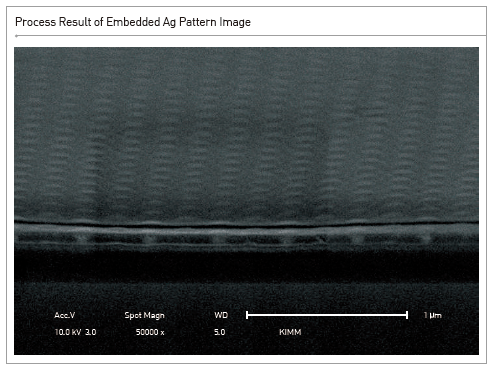
- It is a simple, convenient way to achieve “flattened buried metal pattern formation”
on the optoelectronic devices simply through applying plasmonic nanopatterns:
without a separate flattening process through combining the nanoimprint process
with the metal pattern transfer process.
Excellence of Technology
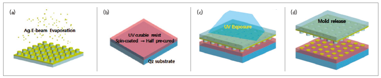
- The bonding layer made of photocurable resin is stacked onto the substrate
- A stamp with protruded patterns, which is to be deposited, needs to be prepared in
advance
- While the thin film layer on the protruded pattern and the adhesive layer are in
contact, pressure is applied on the stamp to selectively transfer the thin film layer
deposited on the protruded pattern onto the above adhesive layer.
- UV ray is irradiated to cure the adhesive layer.
- The stamp is removed.
Current Intellectual Property Right Status
PATENT
- Method of Fabricating Embedded Pattern Using Transfer-based Imprinting(KR1449272, US14 /194,084)
- Method for Fabricating Embedded Metal Pattern (KR1304467)

|