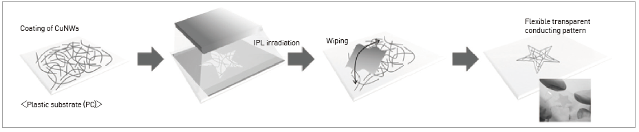
Fast and eco-friendly process and system technology to produce
highly flexible metal (transparent) electrode pattern with simple 3
stages (coating → selective light radiation → wiping)
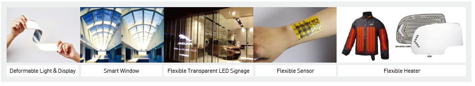
Client / Market
- Deformable light & display, Smart window, Flexible transparent LED signage,
Flexible heater, Flexible sensor
Necessity of this Technology
- Requiring expensive infrastructure such as exposure tool
- Complex patterning process, large amount of chemical waste (PR/etching solution/
developing solution, etc.) and difficulty to apply fast and scalable (roll-to-roll)
process
- Difficult to use metal materials that can easily be oxidized (generally requires
vacuum condition or nitrogen or argon gas atmosphere)
- Issues regarding high surface roughness, low adhesion on the substrate, low
flexibility
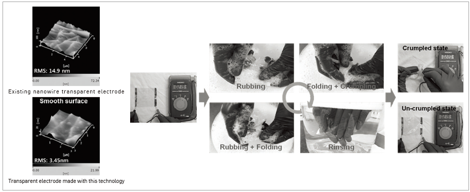
Technical Differentiation
- This system and process can produce highly flexible (transparent) electrode patterns
with high-speed and eco-friendly simple 3 stages without expensive facilities.
- High adhesion on the substrate, low surface roughness can be developed and metal
vulnerable to oxidization in the air can be available
Excellence of Technology
Current Intellectual Property Right Status
PATENT
- Patterning Process Using Photo Sintering on Flexible Substrate (KR1704693)
- System for Conductive Pattern Forming by Light Irradiation on Conductive Metal Ink-Coated Plate (KR1773148)
- Roll-to-Roll Patterning System (KR1821766)
- 5 related domestic, international patents applied
KNOW-HOW
- Large quantity synthesis and refinement technology for metal nano structure (0D, 1D)
- Fabrication of highly dispersed nano conductive ink
- Electrical, mechanical, optical property evaluation technology for printed and flexible film
- Low temperature photo sintering process for various thin films
|