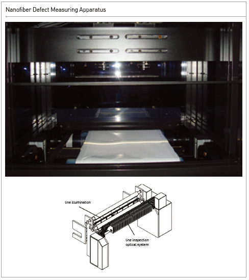
Technology to find defects in the nanofiber web and measure its size and thickness real-time
Client / Market
- Nanofiber, fiber laminating, paper, film manufacturing site
Necessity of this Technology
- Defects in nanofiber web fabricated with electrospinning process has negative effects on nanofiber web’s penetration and filtration function.
- There is a need to test and analyze the nanofiber web’s defects to control the production process.
Technical Differentiation
- Defect detection method: Comparing the intensity of the concentrated light that pass through the defects in the opaque nanofiber web.
- Thickness measuring method: Observing the change in the average intensity of the concentrated light that pass through the opaque nanofiber web.
Excellence of Technology
- Concentrated light is illuminated as a line to minimize noise occurrence and can test the nanofiber web at a high speed.
- Concentrated light is illuminated as a line, and the contrast difference is great between the part with defect and the part without a defect that the location of the defect can be precisely measured.
- The location and number of defects can be measured in real time, and the thickness of the nanofiber web can be measured simultaneously.
Current Intellectual Property Right Status
PATENT
- Apparatus for Monitoring and Repairing of Multi Nozzle Electro Spinning, and Method for Monitoring and Repairing Using the Thereof (Patent registered, 0836274)
- Testing Apparatus of Nanofiber Web and Testing Method the Same (Patent registered, 0893933)
- Apparatus and Method of Checking Defect of Nanofiber and Repairing the Defect (Patent registered, 1056345)
KNOW-HOW
- Measurement variable such as speed, intensity and diameter, etc

|